
CeRAM primer for semiconductor professionals
The physics of correlated electrons has been studied for more than 70 years by physicists and material scientists. Interest in correlated electron materials is accelerating due to the diverse and fascinating properties of these materials ranging from superconductivity to compelling optical properties. At Cerfe Labs, we believe that we have harnessed correlated electron materials, for the first time, to make a practical electrically controlled switching device. Our correlated electron RAM (CeRAM) aims to utilize these unique physics for a superior non-volatile memory. This blog is intended to provide an overview of the unique physics of operation behind CeRAM, for semiconductor engineers.
The field of correlated electronics is not part of the standard semiconductor engineering practice, and even review articles of correlated electron materials are somewhat inaccessible for semiconductor engineers due to a large knowledge barrier. To bridge this gap, we will start with analogies from Silicon technology to provide a common language. If you are rusty with basic semiconductor concepts such as bandgap, doping, electron orbitals, you may wish to see our introductory level CeRAM blog first. After the end of this blog, we recommend additional correlated electron reading material.
Electron Correlation
Electron “correlation” is a measure of influence by an electron on the movement of another electron. For instance, if an electron is already present at a point, bringing another electron in the vicinity of that point will cause a change in the behavior of both electrons due to Coulombic repulsion. A second important “correlation” mechanism is a screening of atomic potential by an intermediary electron. Electron correlation has an energy associated with it known as electron correlation energy and is in a sense related to Coulombic energy due to electron-electron interaction. In real materials, other factors such as ionic potential, core electrons, state quantization, phonons, doping, etc. could affect and contribute to this electron correlation energy.
In most solids, the electron correlation is weaker than the interaction between the positively charged nuclei and electrons. As a result, for semiconductors like Silicon, electron correlation is commonly ignored. We solve Silicon models accurately using what is known as independent electron approximation, which allows us to only consider electron-ion interactions. This approximation works surprisingly well for traditional semiconductors and makes the equations simple to an extent that modern textbooks on Silicon technology do not even mention the electron correlation. On the other hand, for materials such as transition metal oxides, the electron correlation can be comparable to the interaction between the nuclei and electrons. In these materials, the independent electron approximation does not work, and things start to get very interesting.
Correlated Electron Materials
When you consider strong electron correlation in materials, the resulting many-body problems can no longer be solved using simple algebra or even supercomputers. We will need to use approximations, and all of these are semi-empirical fits to experimental data, making the physics of correlated electrons a chicken and egg problem. To understand the properties of electron correlation, we have to rely on experimenting and characterizing materials, but this also makes the entire research time-consuming and a costly pursuit.
This brings us to the genius of Neville Mott and other scientists who predicted and studied correlated electron materials over the last century. Mott studied transition metal oxides which are insulating, when by intuitive understanding at that time they should be metallic, due to a partially filled d-orbital. Mott argued that strong electron correlation was the reason for this discrepancy, and that electron correlation also gives rise to unexpected properties in these materials such as magnetism and ferroelectricity. An insight into why amorphous materials can sometimes behave as metallic and insulting other times won Mott the Nobel prize in Physics in 1977 and due to his initial work, these materials also came to be known as Mott insulators. Mott did many other phenomenal works during his lifetime and, therefore, he is considered one of the greatest and most admired scientists of the 20th century. If you are interested in reading more about his extraordinary life in science, we recommend his autobiography – A Life in Science.
Mott insulators are very different than band insulators that you might be familiar with. For example, crystalline Silicon is a type of band insulator in which electrons primarily interact with the periodic potential of the ions (also known as free particle approximation). The periodic potential allows the representation of electrons in terms of Bloch waves and results in a bandgap. If we break the periodicity in Silicon the Bloch waves no longer exist and the electronic band structure in amorphous Silicon changes drastically. On the other hand, Mott insulators such as NiO are dominated by electron-electron interactions rather than electron interaction with periodic lattice and this electron correlation creates an energy gap.
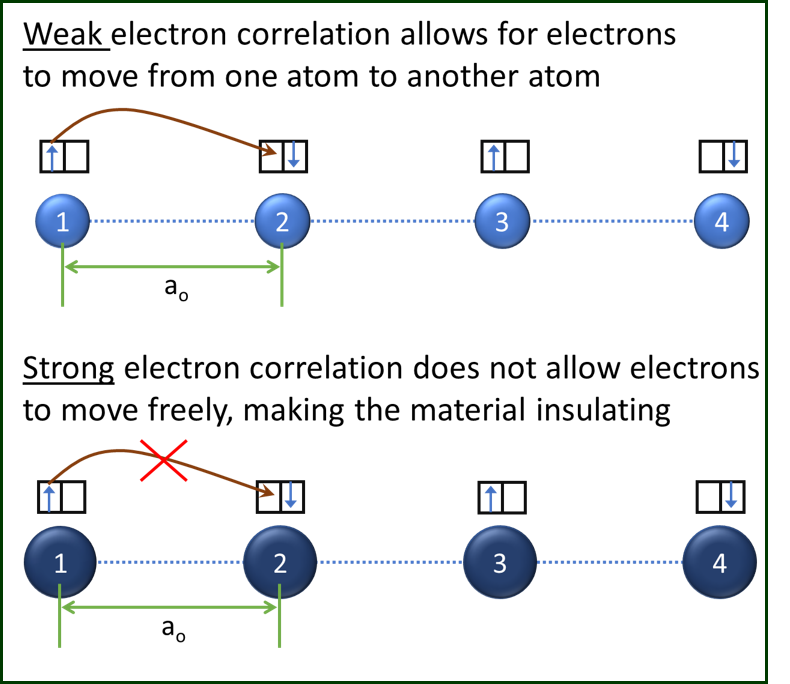
Figure 1: 1D chain models to show the effect of electron correlation on carrier transport. The top atom chain has weak electron correlation, while the bottom atom chain has strong electron correlation. Each atom is assumed to have two available states in the highest energy orbital (shown by the boxes) and one of the states is occupied by an electron, which is shown by an arrow (indicating spin). The other available state in all orbitals is empty, making the orbitals “partially-filled”. Though the representation makes the chain look crystalline, the effect of electron correlation and relevant discussion is equally valid for amorphous solids.
The bottom chain, on the other hand, has a strong electron correlation that prohibits electron hopping from one site to another. As a result, the electrons are “frozen” or ”pinned” or “localized” just like in an insulator. Note that the electron transition through hopping is still allowed under Pauli’s exclusion principle but the energy cost to overcome the Coulombic repulsion is too high, effectively making these materials insulating. As we mentioned earlier, this energy cost for hopping is equivalent to the electron correlation energy. You could also compare this energy to the bandgap in Silicon, for example, where it is possible to excite electrons from the valence band to the conduction band by providing them energy. You should, however, keep in mind that both energies have completely different physical origins i.e., electron correlation in Mott insulators vs. ionic periodicity in band insulators.
Mott’s insight is critical for CeRAM as he had also postulated that the same insulating correlated electron material shown in the bottom chain could be turned metallic if we screen the electron correlation energy. With screening, these electrons will start to hop freely, and the 1D chain will transition from insulating to metallic. Today, we employ Mott’s concepts of strong electron correlation and metal-insulator transition to make CeRAM a reality.
The field of correlated electronics has come a long way since Mott’s discovery with the work of an array of exceptional scientists. John Hubbard later introduced short-range interaction energy between electrons to the tight-binding model and correctly predicted the existence of the Mott insulators as a class of materials that are insulating due to strong Coulombic repulsion between electrons. Specifically, he added correlation energy (U) to account for the repulsion shown in the 1D chain of atoms as a parameter to a simple tight-binding model. His contribution was significant to an extent that these insulators also came to be known as Mott-Hubbard insulators. Hubbard’s model, even though it approximates a complex system, allowed analysis of these strongly correlated electron systems.
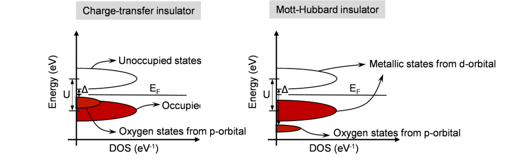
Figure 2: Density of States as a function of energy in insulating state for charge-transfer insulators and Mott-Hubbard insulators. Occupied states are shown in red, while empty states are shown in white.
In addition to Mott-Hubbard insulators, there are similar materials inspired from Mott which are known as charge-transfer insulators. In Mott-Hubbard insulators, the Coulombic repulsion comes from electrons hopping from one metal ion to the adjacent metal ion as shown in the bottom 1D chain example from Figure 1. In charge-transfer insulators, the Coulombic repulsion, also known as charge-transfer energy (Δ), is due to electron hopping between the metal ion and the attached ligand (Oxygen in the case of metal oxides). Interestingly, the first material studied by Mott was NiO, which later turned out to be a charge-transfer insulator and not a traditional Mott-Hubbard insulator. This also highlights the difficulty in predicting the physics of such complex systems.
Figure 2 shows schematics of band diagrams of a charge-transfer insulator and a Mott-Hubbard insulator. In charge-transfer insulators, the top of the valence band is contributed by the ligand or Oxygen p-states. On the other hand, in Mott-Hubbard insulators, both bands are dominated by metal d-states. Note that Mott-Hubbard insulators also have Oxygen p-states, but they are usually deep in energy as shown and do not contribute to conduction or switching.
Going back to the 1D chain analogy, the filled states are now part of the valence band and the empty states are now part of the conduction band. In the case of the charge-transfer insulator with the filled states contributed by the Oxygen (or ligand) p-orbitals, you can easily guess that modifying the ligand, for example by doping and changing the energy levels of the p-states, could change the properties of Mott-Hubbard as well as charge-transfer insulators. In fact, strategic doping of these metal oxides is a key innovation that makes CeRAM possible.
Doping in Strongly Correlated Electron Materials
Although the physics of Mott insulators is understandable to an extent, the response to doping is still an active field of study. It is no surprise that there are very strong and often opposing views in the correlated electron materials community. This is partly because doping a Mott-insulator can lead to unexpected results. For example, doping of cuprates family of Mott insulators will lead to superconductivity or topological insulators or both, neither of which is obvious.
Our aim is not to achieve superconductivity (though a superconducting NVM is not a bad idea) but to enable switching of Mott-insulator using practical electrical signals used in today’s microelectronics hardware. The challenge is that simple models such as Hubbard become intractable beyond a single dimension. There are ongoing attempts to theoretically understand the impact of doping in Mott insulators through the development of advanced theories such as condensed matter field theory. These topics are beyond the scope of the blog post and we will attempt to explain doping in simpler language using the terminologies we have introduced so far.
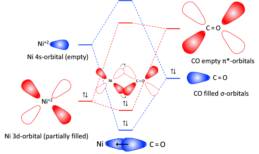
Figure 3: Molecular orbital hybridization during the reaction between Ni ion and CO ligands
When we considered the role of ligands in charge-transfer insulators, we did not discuss the orbital hybridization that might happen when the ligand (in this case oxygen) interacts with the metal ion. Similarly, hybridization also takes place between oxygen p-states and metal d-states in Mott-Hubbard insulators, if they are at similar energy levels. In Figure 2, the p-states of the oxygen are usually shown to be distinct from the d-states of the metal ion, but in reality hybridization results in mixed (or hybridized) dp-states that include features of both p- and d- states. This mixed state can be modulated by the relative strength of the ligand and the metal ion as well as the percentage of the ligand in the compound. The former allows us to choose a type of the ligand based on the strength and the latter allows us to choose doping levels. We can also have a mix of different ligands to make things even more interesting.
Consider the carbonyl ligand introduced in NiO shown in Figure 3. The nickel ion has a partially filled 3d-orbital, while the s-orbital is empty. When CO as a ligand approaches Ni ion, it undergoes orbital hybridization. CO donates a pair of electrons to the empty 4s orbitals making a sigma bond shown in the blue. On the other hand, the Ni ion donates back electrons to CO to make a π bond shown in red. This type of bonding is called π-back bonding and is very common in metal-organic compounds. The resulting molecular band structure shown in the center is strikingly different than the individual band structures. The energy difference between the highest occupied molecular orbital (HOMO) for Ni ion and the lowest unoccupied molecular orbital (LUMO) also changes during the hybridization process. When such doping happens at a large scale in materials, it changes band structure, possibly reducing or increasing the energy gap between HOMO and LUMO of the resulting material.
Reduction in the bandgap of a correlated electron material is equivalent to reducing Coulombic repulsion energy (“U”) or the charge-transfer energy (“Δ”). If we are able to reduce this energy, the work (electrical voltage and current) required to overcome the electron correlation and make the material metallic can be reduced significantly. In our technology, we have observed that the bandgap in NiO reduces from 4.1 eV to a mere 0.6 eV with proper doping. This reduction in band gap is necessary to bring the switching voltages down to practical levels. We have seen a similar reduction in bandgap with HfO, ZrO, YTiO, and other materials.
Doping in correlated electron materials also accomplishes additional utilities such as helping to replace vacancies and passivate defects to provide electrical stability to the oxides which can be amorphous or at least polycrystalline. In the absence of such defect passivation, the vacancies tend to reduce the electrical stability of the oxide, leading to either low-field oxide breakdown or enabling filament formations. We also believe that doping with strong ligands likely changes the octahedral coordination of the metal ion ever so slightly that the dopant is closer to the metal ion due to electronegativity equalization as the bond is formed – further improving the film stability. Such an equalization can further impact the effective electron correlation energy in the material.
If you are coming from a semiconductor technology background, you might be familiar with substitutional or interstitial doping of the order of particles per million (ppm) or particles per billion (ppb). In the case of Mott-like insulators, doping is much higher, to the point where it changes the chemical composition of the material, bridging the gap between doping and alloying. Usually, doping levels are in the range of one-tenth of a percent to 10s of percent.
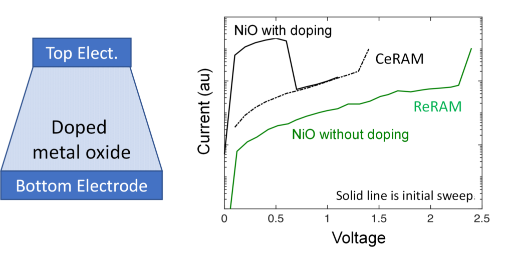
Figure 4: Schematic of a CeRAM device and the switching curve of NiO CeRAM, with and without doping.
CeRAM as a Device
As engineers, we want to move from materials and physics to create a superior NVM device. To make the CeRAM, we sandwich the doped-metal oxide film between two metal electrodes to make a device as shown in the cross-section on the left of Figure 4. This structure enables us to quickly probe various materials developed in our lab and serves as our expected device design of an NVM device. Note that such a structure can be achieved with only three deposition steps followed by an etch step making it extremely simple and cheap. Additionally, we have shown that our technology can be easily integrated into the standard CMOS process flow.
In controlled studies using our MIM prototype devices, we clearly show the importance of doping to enable CeRAM behavior in the case of NiO (Figure 4). For undoped NiO (green curve), you see a low-current insulator with an eventual sharp uptick in current at high voltage, which can be utilized for a resistive RAM device and is a soft breakdown called the forming. At this point, you form a filament and enable the “on” state of the resistive memory.
However, with doping in side-by-side experiments, we change undoped and insulating NiO in green to a “born on” as-manufactured low resistance material (black solid line) that undergoes a sharp transition at 0.6V to an OFF state. This is the reverse of the expected and observed ReRAM type behavior in the undoped NiO. The non-filamentary switching mechanism brings several key advantages over ReRAMs: lower voltage operation, non-polar operation, higher speed, temperature insensitivity, less variation, and scalability to very small dimensions.
Switching mechanism of CeRAM
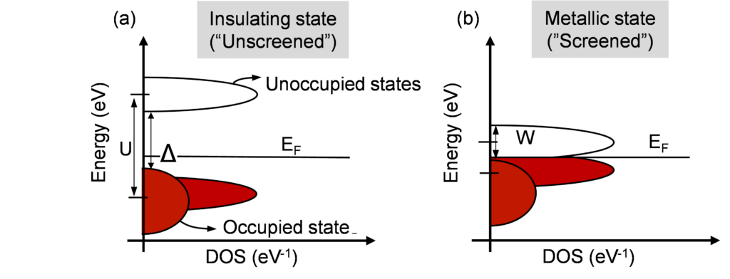
Figure 5: Density of state as a function of energy of Mott-Hubbard insulator in insulating state and metallic state. The occupied states are shown in red while empty states are shown in white.
One of Mott’s conclusions was that it is possible to reduce the effective Coulombic interaction energy seen by electrons by injecting large electron density, which results in the screening of the correlation energy or the U. If we screen or reduce U enough, the material will turn metallic, effectively collapsing the bandgap. The required value of U to transition between metallic and insulating behavior depends on the energy width (W) of the conduction and the valence band. See Figure 5 for a schematic description of U and W.
If U ≪ W, the bands overlap and the material is metallic, while if U ≫ W material will be insulating. Having a small “W”, therefore, helps in making the material switch. The transition or post-transition or post-transition metals have d-states as the highest energy state and the d-states contribute to very narrow conduction and valence bands. These materials are aptly known as narrow-band materials. This is also why most of the discussion regarding Mott-like materials is usually restricted to narrowband materials made out of the transition and post-transition metals.
Silicon for example has a bandwidth of the order to 10 to 20 eV are known as wideband materials. Note that the highest energy orbitals of Silicon are primarily p-states, which are wide in energy. Narrowband materials such as NiO have a bandwidth of the order of 1 to 5 eV. It helps that NiO is a strongly correlated electron material and has a much larger U and as a result, is insulating (U ≫ W) in the as-deposited state as shown by the schematic in Figure 5. Note that CeRAM is different as the ligand doping reduces the bandgap and makes the as-deposited material metallic instead of insulating.
We use strategic doping to reduce the U in the materials permanently to below 1 eV so that the energy required to screen U is not significant. This makes it easier for us to switch this material by injecting charge carriers at practical voltages without breaking down the insulating material. As we increase the charge density inside the material, U gets further reduced due to the screening from the injected electrons following the Yukawa potential model given by Eq. 1.

Where e is the unit electronic charge, r is the distance from a point charge, λTF is the screening length and given by,

Where n0 is the electron density, ϵF is the Fermi energy, and ϵ0 is the permittivity of free space. To effectively screen the electron correlation energy, we need λTF to be smaller than the Bohr radius (aB). Such screening is achieved only at a very high electron density (n0). Mott gave criteria to relate electron density and Bohr’s radius: aB(n0)1/3 ~ 0.25. If n0 is large enough to satisfy this Mott’s criteria, the insulator will transition to metal. Also, while Bohr’s radius is a constant, much like electron mass, just as each material has an effective electron mass, so each material has an effective Bohr’s radius. The Mott criteria are not the same for every material.
The key difference between traditional Mott insulators and our CeRAM technology is the use of doping to modulate the hybridization between the metal ions and the ligands. The switching mechanism concerning screening and de-screening remains the same. In the case of Mott, the as-deposited NiO is insulating due to the Coulombic repulsion. However, in CeRAM, due to the doping, the as-deposited film is metallic with an already collapsed bandgap. We refer to the as-deposited metallic state as “born-on”.
The de-screening in CeRAM is accomplished by extracting electrons from the Fermi level via the application of a pre-defined voltage (energy) – as a result, the unscreened U opens up the bandgap resulting in an insulator state. Once the material has entered the insulating state, we can further increase the voltage to the point where we inject electrons from the metal electrode to screen the U and collapse the bands into the original metallic state and continue this “rocking chair” mechanism repeatedly. Such an ability to electrically screen as well as de-screen repeatedly is one of the key technological achievements of CeRAM.
Non Volatility
For an application as a non-volatile memory, the material must retain the state when the switching stimulus is removed. If we follow Hubbard’s approach, it implies that the thermalization and resulting hopping would lead to 'volatility' or in other words the material will go back to the ground state. To an extent this is true and has been shown, for example, in high-pressure experiments in traditional Mott insulators when the external parameter (pressure) is removed, the metallic phase disappears.
In the case of our doped metal oxides, we observe an initial “born-on” behavior or metallic ground phase that is stable and metallic. This immediately separates it from Mott-Hubbard insulators which have insulative ground states and shows that the Hubbard model does not completely describe our system and needs further theoretical work.
Further, our data show that switching in both directions (metal to insulator and insulator to metal) requires both critical current density (electron density) and critical applied voltage (energy) in such a way that if one is met and the other is not, there will be no phase transition. The sheer robustness of the storage in both metallic and insulating phases is stable up to 400 C for a one-hour bake. This experimental evidence that states are immune against thermal fluctuations or spurious fields and/or currents and are non-volatile.
Our findings are in line with our aim of a superior NVM but at the same intriguing from the scientific point of view. Currently, we can only speculate on reconciling our observations and theory. We do have ongoing collaborations with leading academic groups that we hope will help to shine the light on this.
A History Correlated Electron Materials and Learnings for CeRAM
At Cerfe Labs, we are proud to be the first to venture into making a practical electrically switched device out of correlated electron materials and are committed to bringing CeRAM’s novel physics to an improved commercial microelectronic memory. It is important to consider that non-volatile memory is just one of a wide variety of new capabilities that harnessing these unique materials can provide. Understanding this wider scope, including the history of past research in correlated electron materials helps us to both predict fundamental limits of CeRAM and also paint a picture about future applications beyond the NVM of our devices.
One of the prominent future applications of these materials and also a goal post for the condensed matter physics community is high-temperature superconductors. The state-of-the-art superconductors either require low temperatures or very high pressure and make them unsuitable for large-scale applications. The field of correlated electronics and topological materials promises to make superconductors available at normal conditions of temperature and pressure, and we have early-stage research into this field.
Another application might be closer to realization. Vanadium oxides (VO2 and other stoichiometries) are well-known strongly correlated electron materials that can switch between insulating and metallic phases, similar to CeRAM. Unfortunately, VO2 has a thermal phase transition with a critical temperature around 67 C, where the insulating material transitions to metallic. In very limited applications, heaters have been applied to VO2-based devices to keep their operation above the critical temperature, but that is not something mainstream technology can afford. However, vanadium oxides are an ideal candidate in applications such as electronic static discharge (ESD) or thermal switching.
VO2 has had a long and interesting history, which might need a blog post on its own. It has become popular mainly because the material system is simple (no doping). It is also easy to grow on a variety of platforms and, therefore, one of the easiest materials to study the correlated electron behavior. VO2 has taught the community a lot about the properties of correlated electron materials, which we hope to replicate in CeRAM as well.
First, VO2 switching is extremely fast, of the order of a few 10’s or 100’s of femtoseconds, showing that correlated electron switching has a fundamental switching speed that is much faster than established memory technology. The fastest switching of the order of 100 picoseconds today can be obtained in SRAM memories, which are volatile. One of the promises of CeRAM is that it is the only memory to switch much faster than the best available technology i.e., SRAM while being non-volatile. Established NVM technology such as Flash can take microseconds to write. So far, CeRAM has shown switching down to 2 nanoseconds pulse width for read and write, which has been limited by our testing set up. We have ongoing projects to show much faster CeRAM switching as proof of fundamental speed limit as well as scientific interest. We hope to update the results very soon.
Note that in this short post it is not possible to cover all the exciting research in the field of correlated electronics. We have focused on a subset of topics that is relevant for the CeRAM technology, keeping the information general enough that you should be able to apply the basics to other sub-fields. Within the correlated electron materials research community, it is anticipated that a much wider range of opportunities extends from sensors to optoelectronics.