
Introductory level overview of CeRAM
In this blog, we want to give an introductory level overview of CeRAM for those who are interested but are not trained, semiconductor professionals. (We also have an advanced level review of the technology here). We do rely on some basic concepts such as semiconductor, conductivity, bandgap, volatile vs. non-volatile memory, etc. If are unsure about the meaning of these basic terms, we have also made a blog to define all the basic terms, which you can find here. If something is not clear or you didn’t find what you were looking for, please feel free to send us a question here.
Correlated electrons
The theory behind the physics that predicted semiconductors required a lot of very complicated math. You can imagine when you have 1025 atoms to count, the math gets difficult. To make these physics calculations tenable, some key simplifying assumptions were made. For instance, here is page 4 from one of the main “solid-state physics” textbooks written by Neil Ashcroft and David Mermin: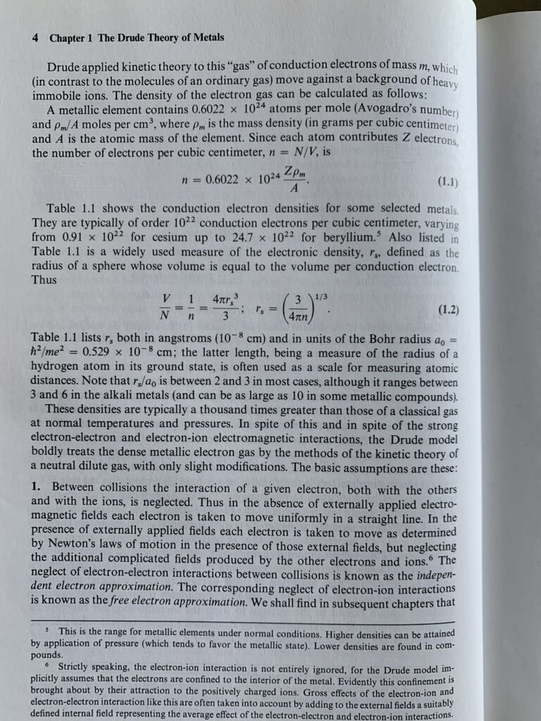
Note toward the bottom the text in italics is “independent electron approximation”, which means that on page 4 of the book (which is considered by many the best on the subject… along with Kittel) we are told to assume that electrons in a semiconductor do not see each other at all. Surprisingly, this simplifying assumption works well in most cases. The physics/mathematics that it facilitates was used to invent the Bell Labs transistor (see background blog), life as we know it changed forever, and physics is still used today in the creation of advanced microelectronics.
All approximations/assumptions eventually run into some problems. As two electrons near each other, their similar negative charges will cause them to repel each other, quite strongly if they get too close, a process known as Coulomb repulsion. For example, in modern highly scaled NMOS, this Coulomb repulsion accounts for a large portion of the drain resistance as electrons leaving the channel to interact with the electrons in the drain. The electrons in the drain push back at these channel electrons which increases resistance. Therefore, if you put enough electrons into a material (i.e. increase the electron density), you can expect their behavior to deviate from the simple textbook equations due to Coulomb repulsion as they are forced to get closer and closer. A second (also Coulombic) issue is that while conduction electrons are “free to roam about” in the material, their behavior is still strongly affected by the electric potential of the atoms that comprise the material. These atomic potentials essentially push and pull the electrons which affects the material’s conductivity. If the electron density becomes high enough, enough electrons can be present around each atomic nucleus that collectively can overwhelm the atomic potential and make it effectively disappear from the point of view of other electrons, a mechanism called “screening”. Screening can cause even stranger effects on the material’s conductivity, sometimes very suddenly.
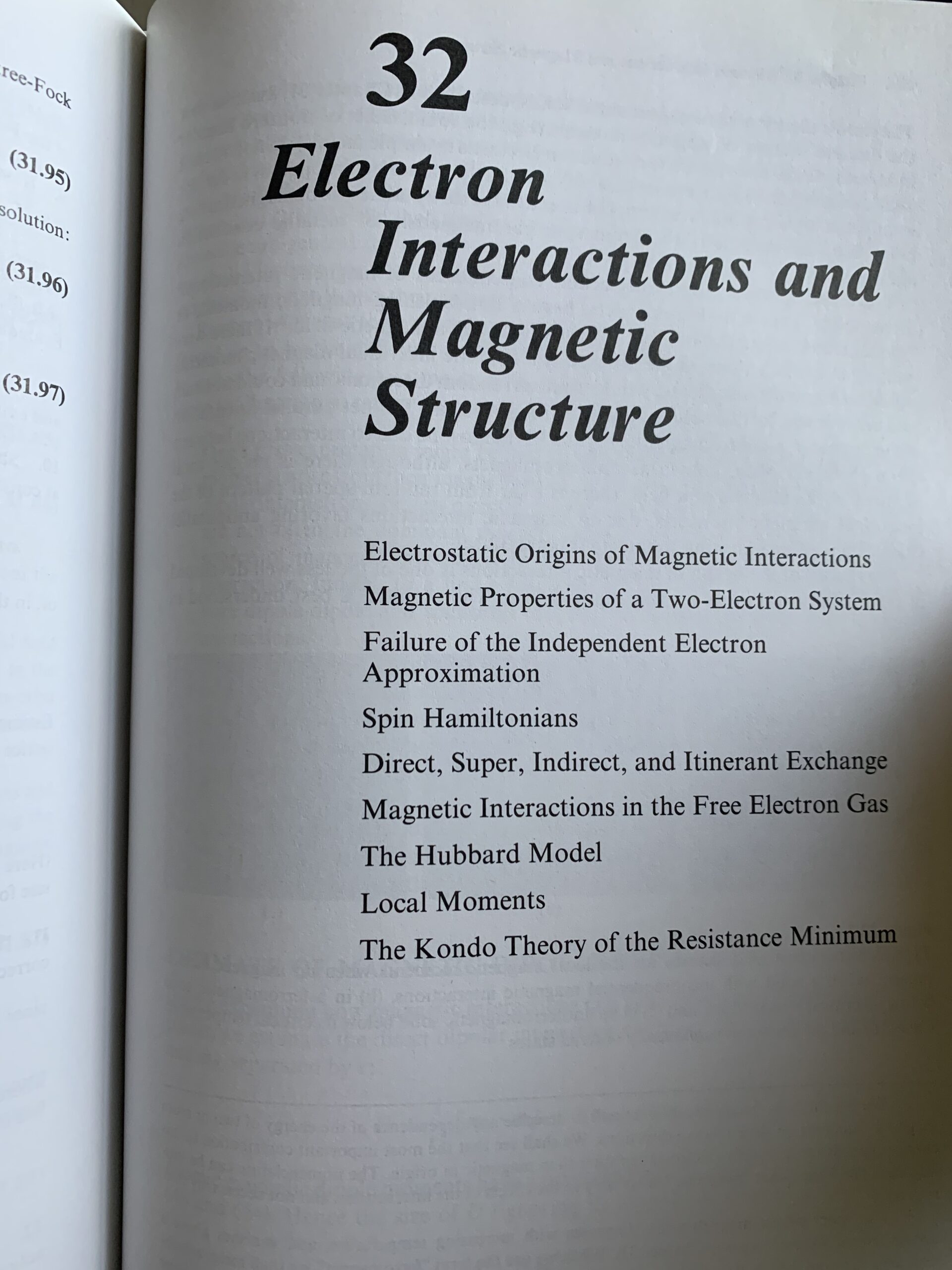 When these two Coulombic interactions (repulsion and electron screening) are strong, the independent electron approximation will break down. Most semiconductor devices (until recently) have not needed to pay attention to these effects. Ashcroft and Mermin get around to discussing these “electron interactions” way back in Chapter 32. You can see in that chapter a section dedicated to the “Failure of the Independent Electron Approximation”.
In 1949, Neville Mott analyzed possible failures in the independent electron assumption, and in so doing he identified specific materials that could possess special properties due to electron interactions, a.k.a. electron correlation. In physics circles, Mott’s concept is considered one of the most important advances in 20th-century physics (Mott would later be awarded the 1977 Nobel Prize in physics).
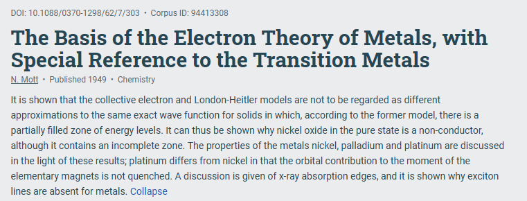
Mott’s original paper, from semanticscholar.org
In particular, Mott identified a class of materials that could undergo a dramatic change in behavior if the average electron spacing became too small (electron density too large), and he calculated specifically how close the electrons need to be for these dramatic changes to occur. This is called the “Mott Criterion”, aB(ne)1/3 ~ 0.25, a very simple formula with very large potential to create revolutionary electronic devices. Mott compared this critical average distance between electrons, to the “Bohr radius”, aB , which is a unit of length that relates to the distance between the nucleus of an atom and the electrons orbiting it, and is a convenient constant for physicists to use (5.291772 x 10⁻¹¹ meters).
 This equation simply states that if the electron density (ne) increases to the point where the electron spacing reaches about one-fourth of a Bohr radius (aB), then weird things will happen. Specifically, a Mott transition can occur in certain materials at this electron density. This Mott transition can be quite dramatic, changing the material from an insulator to metal almost instantaneously. It is important to note that the “switch” in properties does not come from moving electron potentials from valence energy to conduction energy like in transistors, but changing the band structure of the material “on the fly”: collapsing the bandgap from some large value (definition of an insulator) to 0. Instead of doing all the work to push the electrons up to the conduction band, analogous to how hard it is to bend a spoon, Mott identified an easier way, just like Neo did in the movie “The Matrix”.
Mott noted that this Insulator to Metal Transition or “IMT” can be accomplished in certain “transition metal oxides”, which are insulating materials made from oxygen and any of the transition metals in the periodic table. Mott’s original work highlighted the material Nickel Oxide, NiO. In the ensuing years, additional materials were identified, and the field of study broadened from “Mott insulators” to many additional “correlated electron” materials. Of course, the most useful materials are where these electron correlation effects are strongest, so today you most often see the term “strongly correlated electron systems” used in the physics community. Correlated electron switching has been harnessed previously, for instance in devices made from the element Vanadium. Unfortunately, Vanadium oxides have an abrupt transition based on the temperature at about 60⁰C which may sound hot but is in the normal operating range of most computer chips. This is predicted by Mott and verified in real materials, that pressure and temperature can also cause a Mott transition. For electronics, we of course want to control the transitions electrically, and that is the promise of the technology that Cerfe Labs and research partner Symetrix have demonstrated. We have demonstrated the ability to create electrically-controlled correlated electron switches in several different materials, but one is the original material Mott concerned himself with, Nickel Oxide.
CeRAM
It is typically a long path from the discovery of a promising physics concept to the demonstration of useful electronic devices. The first working transistors took decades after physics was understood. Part of the problem at the time was obtaining semiconductor materials at the required purity. The same can be said for correlated electron switches suitable for microelectronics. While temperature and pressure transitions are nice for the study of physics, for microelectronics we need to control devices electrically, and that means connecting the switching material to conducting wires. It is also obvious that we need to be able to switch the resistance in both directions (insulator to metal and then metal back to insulator), but that that has proved elusive in many cases. And finally, we have to accomplish all of this using a manufacturing method that is compatible with the advanced manufacturing techniques that make the continuation of Moore’s Law possible, which is easier said than done. That is a difficult set of requirements, but that is what Cerfe Labs has accomplished with CeRAM.
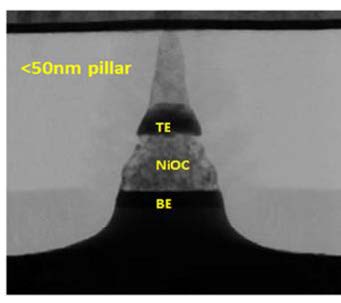 CeRAM is made as a pillar of three materials, which you see in the figure on the right. This picture shows one of these pillars sliced in half vertically and viewed from the side (a cross-section view). The correlated electron material is the “NiOC”, Mott’s nickel oxide, but with our carbon doping technique, that is sandwiched between two connecting metal layers which are called electrodes, a TE “top electrode” and BE “bottom electrode”. In our CeRAM devices, we can push electrons into and out of the correlated electron material through either the top electrode or the bottom electrode (an ambidextrous feature referred to as “nonpolar” operation which can make the device easier to operate) and achieve correlated electron switching transitions via bandgap switching just as Mott predicted.
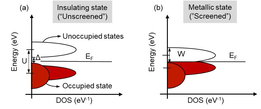 This bandgap transition is depicted on the left, where, at the critical electron density, our material changes from an insulator that has a bandgap (represented by the Greek letter delta, Δ) to metal without a bandgap, by moving the band structure and not the energies of the electrons (Fermi level, EF). A key invention by Symetrix was the discovery that carbon doping reduced the voltage required to achieve a Mott transition in NiO from a large voltage to a much more manageable 1.2V.
We do not know how small we can make CeRAM pillars, but we are confident that it is much smaller than this 50nm example (nm: nanometer, one billionth of a meter). 50nm would already make a bit cell that is smaller than the most advanced SRAM built today. We have demonstrated that we can switch our CeRAM devices from 1’s to 0’s (or the other way around) fast enough to compete with SRAM, which as you recall is a key advantage of SRAM. We have shown CeRAM switching in under 2 billionths of a second or 2 nanoseconds. And in another potentially game-changing capability, our CeRAM can hold more than 1 bit in a bit cell. SRAM cannot do this, but Flash can, which is one additional reason that Flash is the cheapest memory. The SD cards in your phone or Solid State Drives in your laptops give you so much memory for the dollar in part because they can hold 3 or 4 bits’ worth of information in every physical bit cell. To hold 3 bits worth of information, your device needs to be able to reliably provide 23=8 different levels of resistance. CeRAM can do that too, so it is not only that CeRAM can be physically smaller than SRAM, but furthermore, it can store more than one bit in that area, which is why CeRAM will ultimately be much cheaper than SRAM.
Also important, CeRAM is a non-volatile memory, so it can be the “most universal” memory technology: The non-volatility of Flash combined with the high speed of SRAM. This “best of all in one” goal is why we are excited to be developing CeRAM at Cerfe Labs and to demonstrate for the first time the ability to electrically control a bi-directional correlated electron switching device that can be made at a very small dimension. We still have a lot of work to do, but we have proven in prototype devices such as the cross-section shown above that the promise of the physics of correlated electron materials is in hand.
Ce beyond RAM
Oxide Electronics using ultrafast Metal-Insulator transitions: Yang, Ko, and Ramanathan, Harvard
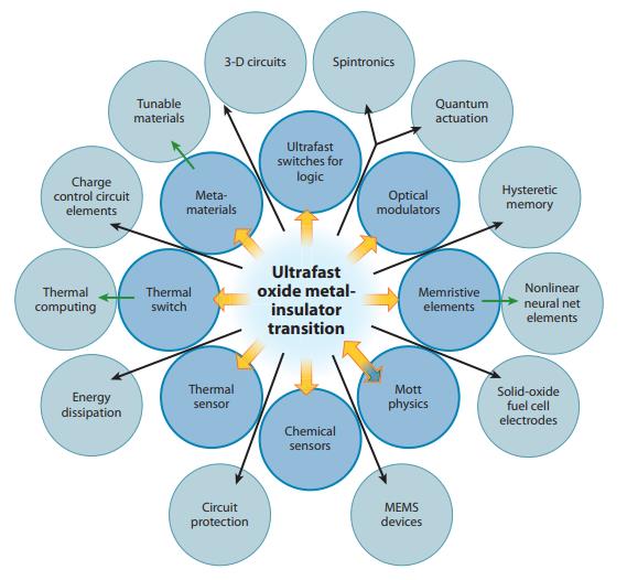
Creating better microelectronic memory is one of our obvious end goals, given that today the market for embedded SRAM, stand-alone DRAM, and stand-alone Flash chips are $20B, $120B, and $80B respectively, and are expected to continue to grow. However, the ability to harness correlated electron transitions in a nanoscale device has many other possible uses and may create new markets with new capabilities. For instance, CeRAM does not need to be made on a rigid silicon wafer substrate, as our materials can be created by ink-jet or other “additive manufacturing” techniques to allow for “flexible electronics” to be placed into bandages, clothing, paper, etc. And correlated electron materials can create additional new opportunities in optoelectronics (already used in high-performance computing and communication), radiofrequency electronics (Wifi, 5G, and Bluetooth are examples), and novel sensors for the Internet of Things (IoT). The many possible opportunities with electrically controlled Ce devices are summarized in this figure by Harvard researchers. At the 2 o’clock point in the outer circle, you see the term “hysteretic memory”, a term for non-volatile memory, which is what we are initially most focused on as noted. However, you’ll note many other possible uses, including at 12 o’clock “ultrafast switches for logic”, the other main use of transistors on computer chips. Correlated electron devices have the potential to be made smaller and faster than today’s transistors, possibly further extending the path of Moore’s Law. As we mature our new company, we expect to add strategic collaborators to help advance the many different promises presented by CeRAM.