
Technical background: CeRAM, semiconductors, and memory
The “Ce” in “CeRAM” stands for “Correlated electron”. Cerfe Labs have harnessed this correlated electron effect to make, for the first time, a practical Random Access Memory (RAM). The electronics world is constantly in demand of better memory, specifically we need more of it and we need it to run faster but use less power. CeRAM’s unique physics of operation delivers on all fronts. Understanding correlated electron physics ultimately requires the use of quantum physics, and we have a blog here for trained semiconductor professionals who can jump straight into that, but we also wanted to provide an introductory overview of CeRAM for those who are interested but are not trained in semiconductor professionals. As we ran this introductory-level blog past non-professionals (thank you, friends, and family), we realized that we could bring this introduction to our technology to a wider audience if we also provided a brief primer on semiconductors and memory terminology. Below we provide key background information such as “what makes a semiconductor” and some background in microelectronic memory terminology. We hope that after the background information below, even if you have very little familiarity with the microelectronics field you can then read our introductory level CeRAM blog and share in our excitement about this new technology. It is of course a reach to think we can cover this very complicated field in a few paragraphs, so if something is still not clear or you didn’t find what you were looking for, please feel free to send us a question here.
Background terms: electrons in materials
Most materials fall into one of three categories based on how the electrons behave in the material. If you roll back the clock enough, there were no “solid-state” materials, just clouds of atoms. When these individual atoms came together to form chunks of material (“condensed matter” in physics textbook terms), in some cases all of the electrons remained bound to the atoms, while in other cases some of the electrons ended up unattached to their atoms to roam around freely in the material. These two types of materials are called insulators and metals, respectively. Insulators do not conduct electricity because none of the electrons are free to move, while metals can easily conduct electricity because there is a sea of mobile electrons in them. Gold, copper, and aluminum are the metals (a.k.a. “conductors) that form most of the wires in your electronics, while glass, paper, and plastics form most of the insulators that keep the wires isolated from one-another (spark avoidance). A related factoid: metals are generally cold to the touch because the free electrons are good at dispersing heat.
The computer chip industry is built on the third class of materials. These are the Goldilocks class of materials called “semiconductors”. Semiconductors are insulators at heart and do not conduct electricity when cold and in pure form, but they are weak insulators and clever engineers figured out that semiconductors are reliably tuned chemically to create useful devices that can switch their “conductivity” between a good-enough metal and a good-enough insulator. Useful electronics rely on the ability to make a device that can switch resistance on demand. Semiconductors, then, are materials that can be made to change their “resistance”, the electronics term for how easily electrons move through a material, both chemically and via applied voltages.
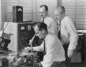
John Bardeen, William Shockley, and Walter Brattain at Bell Labs in 1947. [bell-labs.com]
Electronics made from chunks of semiconductors were a big breakthrough compared to the devices they replaced, electro-mechanical relays and vacuum tubes because these new “solid-state” switches (as opposed to vacuum tubes that require seals or relays with physically moving armatures) had vastly superior reliability and (eventually) could be made really, really small.
One of the big discoveries that ushered in the modern electronics era was a solid-state device that used an electrical input wire to change the resistance between two other electrical wires: a “transfer resistor”, concatenated to “transistor”. This discovery earned William Shockley, John Bardeen, and Walter Brattain (pictured) of Bell Labs the 1956 Nobel Prize in physics. The device shown below is their breakthrough discovery. The triangle lined with gold foil is a “point contact” pressing down onto a bar of germanium, which is a semiconductor.
To nudge a semiconductor’s resistance, one can “dope” a semiconductor material, introducing low levels of impurity atoms that turn it into a decent conductor. The “p-type” and “n-type” regions in the germanium of the Bell Labs transistor are areas where they doped the germanium to give it slightly more or fewer electrons than normal (negative type vs. positive type, where electrons carry a negative charge).
The photograph of noble prize-winning point-contact transistor (left) and the schematic showing the details of the device. [bell-labs.com, Wikipedia]
An easier way to turn a semiconductor into a conductor is to shine a light on the semiconductor. This “feature” is why solar panels are also made from semiconductors. Finally, one can push the electrons away from the atoms and into the free-flowing state by applying voltage. Voltage is the potential energy of electrons pulled by electric fields, somewhat analogous to the way height is the potential energy of objects that are pulled by a gravitational field.
We mentioned earlier some electrons get stuck near their atoms and then some electrons are free to roam about the material. Due to the underlying physics, there is a set of energies where the electrons stuck near the atoms (called valence electrons) exist and a different (higher) set of energies where the electrons that can roam around the material (called conduction electrons) can be. These energies are tightly arranged into “bands”.
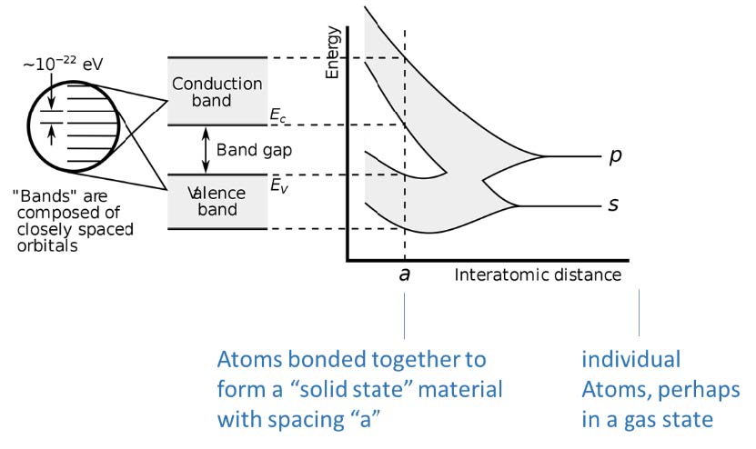 The picture here illustrates the concept we started with, where you imagine atoms starting far away from each other at the right of the pictures (large “interatomic distance”) and then approach each other to eventually form a solid material with spacing “a”. When they are individual atoms in the gas state, the two-electron states have distinct energies “p” and “s”, but as they get near each other, quantum physics interactions dictate that the energies expand into a range of energy “bands”, where for some materials the bands merge and for some materials, the bands split and leave us with a bandgap.
For semiconductors, the Goldilocks property comes from a bad gap between the valance band and the conduction band that is just big enough so that if we want the material to be an insulator (“off” in terms of an electronics state) we can keep the electrons in the valence band, but the gap between the valence band and the conduction band is small enough that we can use one or more of the nudging techniques to get enough electrons up into the conduction band switch the material into a conductor when we want. A bandgap of 1 or 2 volts is a convenient voltage that can be supplied by batteries, for instance. As an aside, you can give enough energy to the electrons by shining light on them: the incoming photons impart enough energy to valence electrons that they can rise and turn into conduction electrons. That is the principle that makes solar panels possible.
If the bandgap is too large, the material is an insulator because it takes an unreasonable amount of energy to push electrons up into the conduction band. Metals have no bandgap, or even a negative bandgap, i.e. the two bands overlap (see picture below).
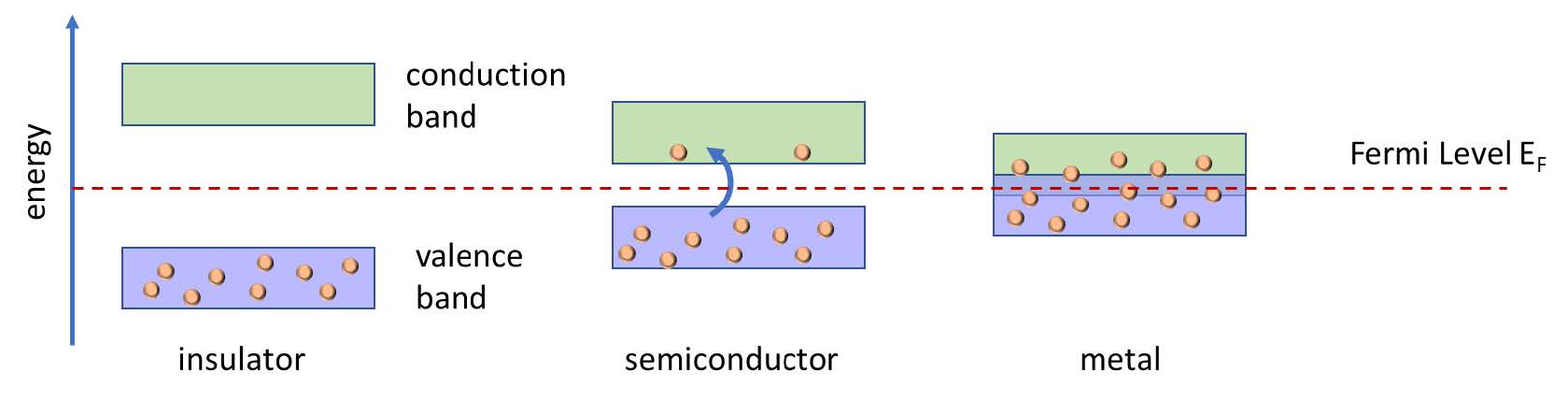 This picture introduces the key semiconductor term Fermi level, which for the sake of simplification is the energy above which electrons can be free to roam about (conduct electricity). That Fermi level does not have to be centered between the bands, a fact that we exploit when designing transistors. An analogy for the Fermi level is the level of the top layer of ping pong balls in a box. If you jostle the box hard enough a few of the ping pong balls will get just the right energy to pop up high enough to leave the box, in this analogy changing from “valence balls” to “conduction balls”.
Temperature also acts as a source of energy to the movement of atoms and electrons, and even at a mild room temperature, some electrons can get bumped across a small enough bandgap to become conduction electrons (blue arrow in the figure above). So for practical electronics, we’d like a bandgap comfortably above 0 but not 5V because moving electrons up and down across large voltage ranges requires extra energy. Silicon’s bandgap is a Goldilocks 1.1V, so valence electrons won’t jostle up to the conduction band at room temperature, but with reasonable effort, we can nudge them up there when we want to, changing the insulator into a conductor. The integrated circuits we use in all electronics are simply collections of tiny transistors that are turning their conductivity on and off by moving around the Fermi level of the semiconductor materials from which they are made.
Semiconductor memory
| Computer information is stored in the “binary digits” 1 and 0, a phrase that was quickly concatenated to the term “bits”. A location on a computer chip that holds a bit is called a “bit cell”. A group of 8 bits is called a “Byte”—the y in byte does not come from any special meaning…a very smart engineer foresaw that if engineers were typing both “bits” and “bites” there would be mass confusion based on typos, so he changed the spelling of bite to Byte. 1 Byte of memory can represent 28 or 256 different values. Notice also that we keep bits as lower case b and Bytes as upper case B: something to pay attention to, as 1kb (one thousand bits) is eight times smaller than 1kB (one thousand Bytes) |
Integrated circuits arrange these transistors to process and store information. The processing aspect is called “logic” and the storing aspect is called “memory”. The information is stored in spots on the computer chips called bit cells (see inset) where we have pushed electrons around to create either a lack or an abundance of electrons in that particular spot. These two “states” of memory correspond to the 1’s and 0’s that make up all of the information in the computer. The technologies vary by how they write 1’s and 0’s into the bit cells, and how the bit cells store the information for later, but all of these memory technologies ultimately “read” the value of the bit as a high or low resistance (which is how much current you get when you apply a voltage—the first key equation in Electrical Engineering 101 is that voltage = current x resistance).
As wonderful as our electronics are these days, there is always more we could do if we could process the information (move the electrons around) faster, do it with less energy (drain your phone’s battery a bit slower), and make the computer chips at a lower cost (put more memory into the same priced chip). That cost aspect has been the wonder of the semiconductor industry, which has for over 50 years roughly doubled the number of transistors per chip every two years, a feat referred to as Moore’s Law. And it turns out if you make the circuits smaller, you need fewer electrons to create a voltage (saving power) and the electrons don’t have as far to travel from one part of the circuit to the other (increasing speed).
A looming problem that the semiconductor industry is facing is that it is increasingly harder to make the bit cells smaller, or move electrons in and out of them any faster, using any of the big three memory technologies, SRAM, DRAM, or “Flash” EEPROM (acronyms explained below). The reason we use three different technologies is that none of them are universally great at being fast, cheap, and low in energy use. For this reason, computer “architects” design very complicated mixes of these three technologies to create the memory system for a laptop, phone, etc.
SRAM is the fastest of the three but also the most expensive, so we use it sparingly near the logic transistors on the processor chips. We call memory that is on the same chip as the logic processor “embedded memory”. By “sparingly”, we can usually pack a few million bits (mega-bits, Mb) onto a processor chip. Expense in computer chips is mostly about the area, and SRAM requires 6 to 8 transistors to form one bit.
DRAM can be made much more cheaply because it requires just one transistor and one capacitor, but only if we make the DRAM on separate dedicated chips (which we call “stand-alone” memory). To use a stand-alone memory, we pay a penalty in speed (and energy) to move electrons from the processor chip to the DRAM memory chip where we can have a lot of bits, and then back when we need it. Modern DRAM chips hold billions of bits, or gigabits (Gb).
Both SRAM and DRAM are “volatile”, meaning they will forget their information if you turn off the power to the chip. The D in DRAM stands for a brilliant marketing term “Dynamic” which means that DRAM is perpetually in the process of forgetting the information even when the power to the chip stays on—the DRAM’s memory has to be refreshed a thousand times per second to keep it from forgetting.
Computer information is stored in the “binary digits” 1 and 0, a phrase that was quickly concatenated to the term “bits”. A location on a computer chip that holds a bit is called a “bit cell”. A group of 8 bits is called a “Byte”—the y in byte does not come from any special meaning…a very smart engineer foresaw that if engineers were typing both “bits” and “bites” there would be mass confusion based on typos, so he changed the spelling of bite to Byte. 1 Byte of memory can represent 28 or 256 different values. Notice also that we keep bits as lower case b and Bytes as upper case B: something to pay attention to, as 1kb (one thousand bits) is eight times smaller than 1kB (one thousand Bytes)
To keep all the cat pictures on your phone safe when your battery runs out of juice, we use the 3rd type of “Flash” EEPROM memory which is a “non-volatile” memory (NVM), meaning the bit cells will retain their information even when the power is turned off. EEPROM started as a simple acronym, Read-Only Memory (ROM), but then someone figured out how to make ROM “Programmable” so there became PROM, and then someone else figured out how to make the PROM “Electrically Erasable” resulting in EEPROM, and then finally someone figured out how to make the erasing function happen with a flash of light, ending with “Flash EEPROM”, where now the EEPROM part is often omitted. Flash memory is the cheapest of the three because it can be made with just one transistor, but very slow, especially to write information into it, and a tad power-hungry. The “SD” type cards you can insert into your phone are made from Flash memory, as are the “Solid State Disk” SSD drives in your laptops (yes, Flash memory is slow, but compared to a hard disk drive they are fast!). Because Flash memory is the cheapest, we can afford to put over a trillion bits (tera-bits, Tb) into the SD cards and SSD drives. Unfortunately, Flash memory wears out relatively quickly. “Endurance” is the term used to describe how many times you can write and erase the memory before it starts to wear out. Various Flash memory products are specified to last from 100 to 1 million writes/erase cycles, and we’re betting that you have probably owned an SD card that stopped working at some point.
SRAM’s ability to provide twice as many bits per chip every two years has already fallen behind Moore’s Law, and DRAM and Flash memory technologies are expected to also start slowing down. For this reason, the electronics industry is hunting for better underlying technologies, all of which are lumped into the term “emerging” memory. Cerfe Labs’ research team identified CeRAM (invented by Symetrix Corp.) as the emerging memory technology with the most promising fundamental abilities to simultaneously provide the cost, speed, and low energy required by future electronics. While at Arm, we began an ongoing partnership with Symetrix to develop this technology further, and that partnership continues with the formation of Cerfe Labs. Part of the advantage of CeRAM is that it uses an entirely different physical concept to store information than the semiconductor-based memories that power today's electronics. CeRAM uses “correlated electron” materials to create its advantage. Now that you have this introductory glossary of terms under your belt, you are ready to read our introductory CeRAM blog.